
Mintek owns a JEOL JEM-2100F, Field Emission Gun (200kV), Transmission Electron Microscope (FEG-TEM) capable of providing high spatial resolution, atomic imaging and micro- and nano-structure analysis of materials.
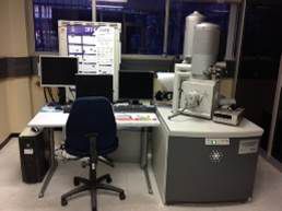
Our FEI Nova Nano-SEM 200 Field Emission High Resolution Scanning Electron Microscope (HRSEM) enables both high and very low kV imaging and analytical capabilities of specimens in and below lens configuration with the option to operate in either high or low vacuum conditions. It is equipped with an Everhardt Thornley Detector (EDT), backscattered electron detector (BSED), through-the-lens detector (TLD) for high resolu-tion imaging, as well as a X-ray spectrometer (EDXS) for X-ray analysis.
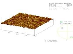
Mintek-NIC owns the Nanoscope and Enviroscope multimode Atomic Force Microscopes. Our multi-mode AFMs uses both contact and tapping modes to analyse samples with the resolution in the nanometer range.The samples can be analysed under high vacuum and conditions like temperature can be altered whilst the analysis is performed.
Various metal and metal oxide nanomaterials are available:
* Various gold (Au) nanorods
* Various iron oxide (Fe3O4) nanoparticles ranging from 4 - 30 nm
* Various gold coated iron oxide (Fe3O4@Au) nanoparticles
* Various silver (Ag), platinum (Pt) and palladium (Pd) nanoparticles
* Various zinc (ZnO) and copper oxide (CuO) nanoparticles
** Custom nanomaterials can be produced on request
The group also produces copper (Cu) and nickel (Ni) grids for TEM application.